[Recommendation] Industrialization of 2 inch single crystal diamond substrate and its key equipment
1. Project Introduction
Excellent properties of diamond single crystals in electricity collection, optics, mechanics and thermals, in high temperature, high frequency, high efficiency and high power electronic devices, biosensors, solar blind UV and particle scintillator detection and imaging, optoelectronic devices, aerospace and weapons The system and other aspects have great application prospects and are known as "the ultimate semiconductor." Diamond electronic devices have higher efficiency (about 18% increase), lower loss (about 30% reduction), smaller size and higher integration than other semiconductor devices, and do not require a cooling system. Its energy consumption is about 1/5-1/3 of the existing devices.
At present, Japan, the United States, Europe, and China have invested heavily in the establishment of relevant organizations and production, research and research institutions to promote the development and application of diamond single crystal materials and their electronic devices. The industrialization of inch-inch single crystal diamond substrate and its key equipment can greatly promote the revolutionary transformation of China's semiconductors, realize the leap-forward development of China's microelectronics industry, and reach the international advanced level.
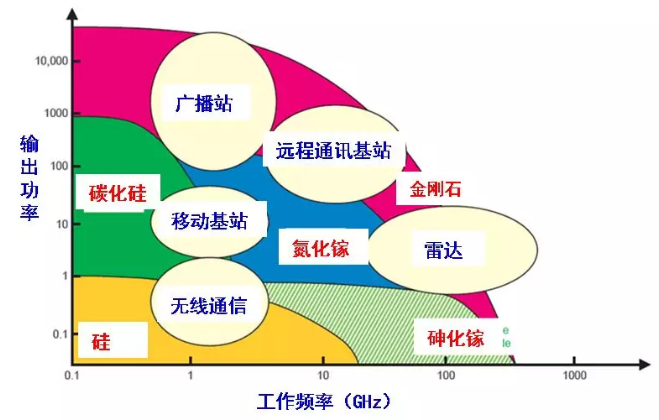
Figure 1 Diamond semiconductor characteristics
2. Product performance advantages
(1) Basic principles and key technical content
The growth kinetics of diamond MPCVD was studied by epitaxial growth of single crystal diamond semiconductor substrate;
Optimize the design of the MPCVD reaction chamber structure to achieve large area, high density and homogenization of microwave plasma;
Optimize the thermal field distribution and airflow distribution of the reaction chamber;
Using the equivalent crystal plane characteristics of single crystal diamond crystals, the lateral growth technique during epitaxial growth is studied, and the diamond substrate with an area of ​​10×10 mm 2 or more is obtained by epitaxial growth of mutually perpendicular crystal planes;
The related laws and methods for forming non-diamond layer under the superficial layer of diamond by high-energy ion implantation technology are studied. The homogenous diamond single crystal substrate with surface layer separable is obtained, which creates conditions for the "cloning" of diamond single crystal.
The crystal fusion mechanism and law of substrate contact in different crystal orientations were studied, and a single-crystal substrate with a larger area was epitaxially grown by patch-fusing fusion to meet the mass production requirements of a 1-inch large-area single crystal diamond substrate.
(2) Innovation points
The process specification of large-area single crystal diamond growth is formed by the method of equal crystal plane and mosaic fusion, which can produce single crystal diamond substrate and film products of 1 inch (25.4Ñ…25.4 mm) or more.
The overall technology for mass production of large-area single crystal diamond by cloning technology was obtained.
3. Market prospects and applications
According to the predictions of Japanese companies, with the development of diamond semiconductors, China's market size reached 10 billion US dollars in 2030. Since the main cost in diamond production is the cost of methane, hydrogen and electricity consumption, the cost is low and the economic benefits are significant. The team owns a complete set of independent intellectual property rights of MPCVD equipment, and the single crystal diamond substrate material is manufactured. The power density has surpassed that of Japan, Italy and other countries. In terms of size, the team can provide centimeter-level (1cm*1cm) products, also international. Advanced level. Although there are inch-level and 2-inch products in the world, they are still in the stage of scientific research, and the output is extremely low, which cannot be industrialized.
The products developed and industrialized in this project and their market applications include the following aspects:
(1) Diamond single crystal substrate
Large-area single crystal diamond substrates are mainly used to develop and industrialize the following diamond electronic devices to provide epitaxial growth substrates:
High-power diamond power electronic device: It can replace the existing Si, SiC and other power conversion devices and switching power supplies, greatly reducing the size of the conversion device, and without heat dissipation, achieving a significant increase in conversion efficiency and a significant reduction in power consumption, reliability Significantly improved. The energy consumption of diamond electronics will be 1/3-1/5 of the devices currently in use.
UHF high-power diamond electronic devices (microwave, millimeter wave radar): can be used in fire control weapon systems, radar, high-speed wireless communications, rockets and aerospace. It can replace the traveling wave tube used now, which makes the weapon system and communication system more compact and reliable, greatly increases the data transmission rate of the communication system, and greatly reduces the weight, launch cost and anti-irradiation of satellites and other spacecraft. ability.
Applied to integrated circuit chips: The development of diamond-based next-generation integrated circuit chips, completely solving the problem of integrated circuit thermal bottlenecks, making integrated circuits larger and faster.
Diamond UV LED, LD: can be used in environmental protection and medical sterilization, high-density data storage.
Biosensors such as DNA: Develop a variety of diamond biosensors using the affinity of diamonds and biological cells and the high sensitivity of biosensors. At the same time, they can also be made into biological weapons detectors.
Sunblind UV detector and ultra-fast particle radiation scintillation detector: used in missile guidance and early warning, deep space x-ray communication.
Other electronics and sensors.
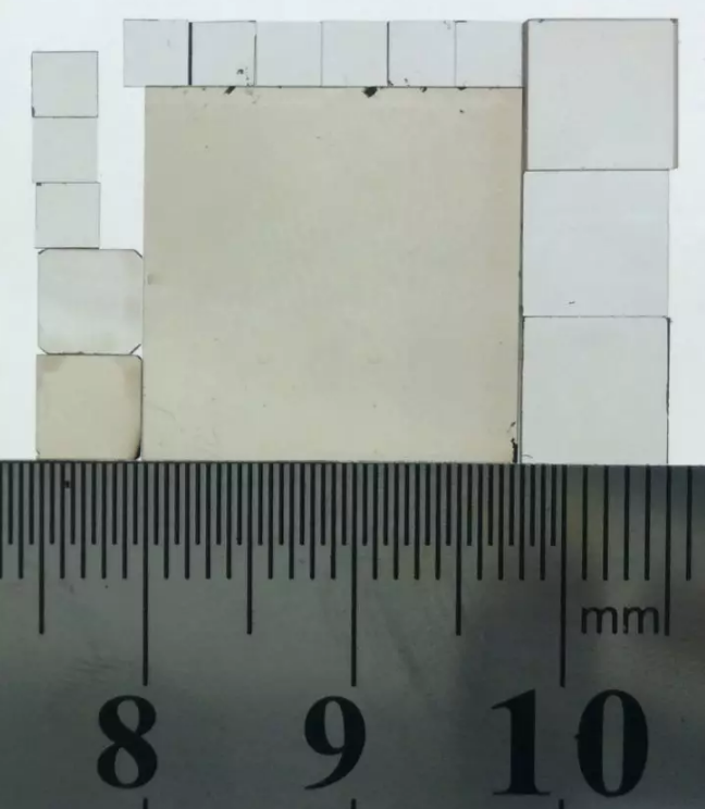
Figure 2 Single crystal diamond substrate
(2) Anti-high-energy microwave and wear-resistant window materials for fighter aircraft and other weapon systems
Using the high-transmission characteristics of the far-infrared to deep-UV of diamond, high thermal conductivity and high-strength characteristics, it can be used to make windows for high-power microwave weapons, long-range guide windows and detector windows.
(3) Superhard material tools
Diamond has the highest thermal conductivity and Young's modulus, and is the hardest material to date, which makes diamonds widely used in tool industries such as tools. For example, the processing of Apple's iPhone in the United States requires a large amount of single crystal diamond, as well as drill bits for petroleum exploration, precision machining of cutter heads, scalpels, and so on.
(4) Microwave plasma CVD equipment
A large number of applications in the above aspects require the use of MPCVD equipment. Therefore, after the development of the diamond electronic device and the military market, the demand for MPCVD will also rise sharply.
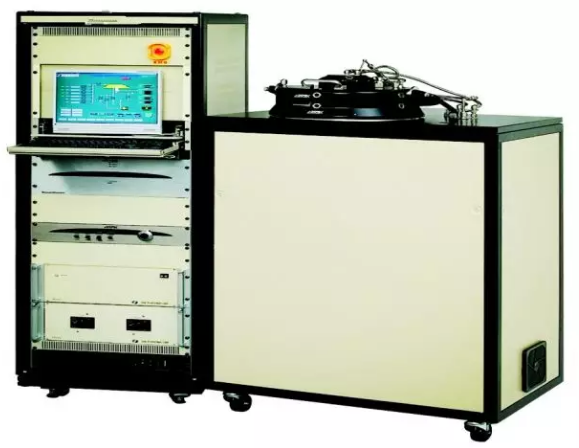
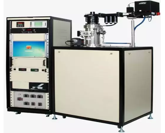
Figure 3 key equipment - MPCVD
(5) Power electronic devices (wide tight band, high voltage resistant, anti-breakdown)
(6) Cultivating diamonds
4. Technology maturity
Mature technology and industrialization.
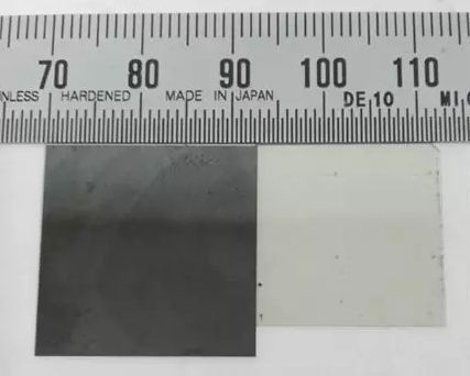
Figure 4 "Cloning" growth of single crystal diamond substrate (before peeling)
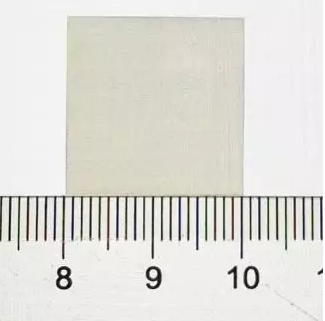
Figure 5 "Cloning" growth of single crystal diamond substrate (after stripping)
Person in charge: Wang Hongxing
contact number
E-mail: u.edu.cn
School: Xi'an Jiaotong University School of Telecommunications
Magnetic Pump have the magnetic seal, pump no leakage, safety, stable operation. Widely used in chemical industry and food industry. we have Magnetic Gear Pump, magnetic centrifugal pump, magnetic Screw Pump and magnetic rotor pump. base on all kind of pump's properties, pump be installed a magnetic coupling, the conveying medium has no leakage and the working environment is clean and tidy. No need to change the seal, easy to use and easy to operate. Depending on the medium being transported, the working environment is different and different pumps are selected.
Magnetic Pump,Magnetic Water Pump,Magdrive Pump,Mag Drive Pump
Hengshui Yuanhan Trading Co.,Ltd , https://www.yuanhanpump.com