Ningbo Materials successfully developed a three-dimensional micro/nano structure manufacturing system
 |
Three-dimensional "write-type" micro-nano structure manufacturing system - preparation table
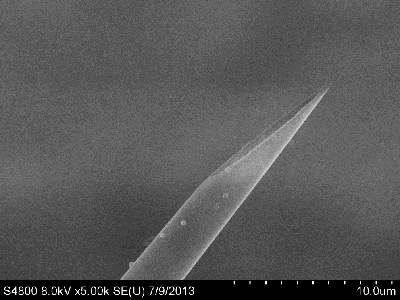
Pen tip shape of "writing" equipment
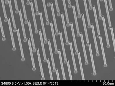
Copper wire array prepared by "writing" platform
Nano-manufacturing technology is the basis for the production of nano-structures, devices, and systems. It takes the micro-nano device manufacturing requirements or key technologies as the traction, solves the key technical issues such as the design, equipment, processes, and applications of micro and nano-fabrication, which is to enhance the nano-manufacturing technology. The essential. Especially with the development of three-dimensional chip manufacturing, three-dimensional information storage, bionic intelligent materials, metamaterials, and MEMS devices, the traditional processing technology is increasingly difficult to meet its development needs. It is increasingly important to study new three-dimensional micro/nano processing technologies.
In order to facilitate the realization of the three-dimensional synthesis of materials and devices in micro-nanometer dimensions, it is now possible to achieve a high level of integration and versatility. The Xu Gaojie Research Team of the Ningbo Institute of Materials Technology and Engineering, Chinese Academy of Sciences, worked closely with Prof. Yu Minfeng of the Georgia Institute of Technology in the United States to successfully develop a “write-through†3D micro/nano structure fabrication system, which realizes micro/nano level single wires and arrays of metallic materials. The rapid growth. At present, the micro/nanowire growth rate can reach 1.3μm/s, which is several orders of magnitude faster than the typical deposition rate of thin films.
The system combines electrochemical deposition with a helium pen process. After the electrolyte comes out of the electrode, it is directly reduced and solidified, and a high aspect ratio (above 100) micro-nano structure can be formed. Using automated control techniques, complex three-dimensional structures and arrays can be easily fabricated. Compared with the prior art, the “write-through†electrochemical deposition technology has a simple process and is easy to operate, can effectively reduce the size of integrated circuits and microelectronic devices, and facilitates the integration of more functions in micro-nano devices.
The liquid-phase “write-through†technology can be completed at room temperature and pressure, and can perform nano-pattern deposition and complete nanolithography; it can also perform nano-structure molding to complete the fabrication of nano-functional devices; it can also be applied to basic nanomaterials. The unit is controlled to complete the nano-integration and is one of the important means to meet the manufacturing requirements of bio-nano devices, bionic systems, large-area flexible optoelectronic devices and systems. This technology can be used not only for the preparation of high-frequency terahertz antennas and precision sensors, but also for the long-distance and obstacle-free interconnection of micro-devices. It can also be used to synthesize new materials such as single crystals or polycrystals. If an array-type pen tip is used, this technique can combine batch preparation techniques with micro-nano scale effects of materials and facilitate batch preparation.
The research work was supported by the Chinese Academy of Sciences Wang Kuancheng Research Prize project, the Ningbo Science and Technology Innovation Team, and the Ningbo Natural Science Foundation.
Cosmetic Pouches,Travel Barrel Cosmetics Pouch,Waterproof Travel Cosmetic Pouch,Pvc Cosmetic Pouches
Dongguan C.Y. RedApple Industrial Limited , https://www.hpgbags.com